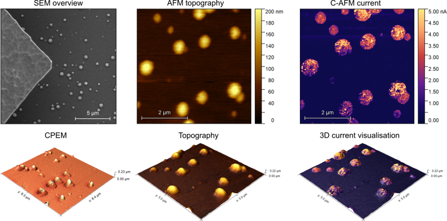
Conductivity of microcrystalline Si

Microcrystalline silicon and Si thin films are used in optoelectronics (solar cells, thin-film transistors, flat panel displays). Therefore, electrical conductivity is likely mandatory in order to understand their potential application or for quality control.
In this case, the complex in-situ analysis provided a local current map, electronic defects, and electric properties in dependence on surface morphology by AFM-in-SEM technique.
Measurement modes: C-AFM
LiteScope benefits:
- Easy structure localization and Tip Navigation
- In-Situ conditions: combined conductivity, topography and material contrast analysis
Courtesy of Aliaksei Vetushko, Institute of Physics, Czech Academy of Sciences
See also

Want to discuss your own application ?
