Inside the Chip: Semiconductor Failure Analysis with AFM-in-SEM
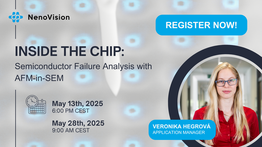
Dive into the world of semiconductor failure analysis and discover how integrated AFM-in-SEM technology enables in-situ, high-resolution electrical and topographical characterization - right where it matters most.
Learn how LiteScope transforms traditional workflows by combining SEM, FIB, and AFM techniques into a single, efficient process - streamlining diagnostics and revealing the root causes of device failure with nanoscale precision.
This webinar will walk you through real application examples, including dopant profiling of MOSFET transistors and conductivity mapping of complex semiconductor structures.
Register now:
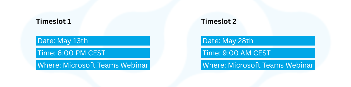
We’re running this webinar twice for our global audience - pick whichever timeslot fits your schedule the best!

Questions?
Webinar
|
16. 04. 2025
|
by Lea Olekšáková
Semiconductors
Product
Related posts
Webinar
|
02. 01. 2025
|
by Lea Olekšáková
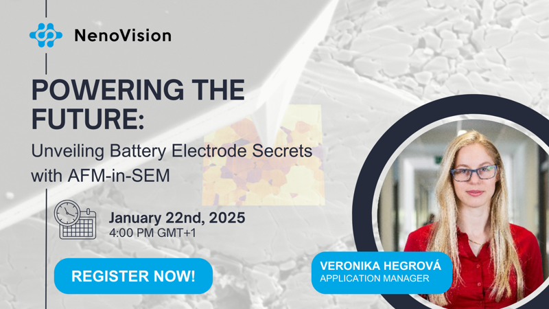
Upcoming Battery Webinar | Unveiling Battery Electrode Secrets with AFM-in-SEM
Semiconductors
Technology

Webinar
|
19. 08. 2024
|
by Markéta Součková
Upcoming Webinar: Battery Component Materials AFM-in-SEM Characterization
Material Science
Product
Technology

Webinar
|
30. 04. 2024
|
by Patrik Maňas
Upcoming Webinar: AFM-in-SEM LiteScope, Redefining In-Situ Correlative Analyses
Material Science
Product
Technology
Webinar
|
15. 11. 2023
|
by Markéta Součková
A webinar on the characterization of Battery Materials
Material Science
Product
Technology
Webinar
|
02. 10. 2023
|
by Markéta Součková
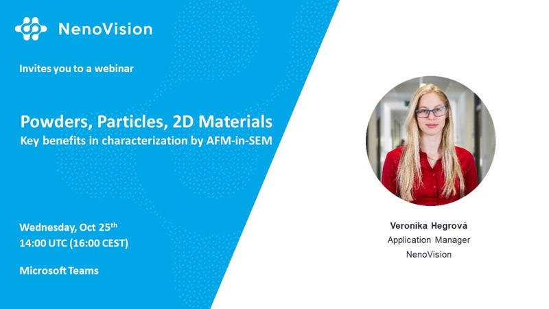
A webinar on the characterization of Powders, Particles, and 2D materials by AFM-in-SEM
Material Science
Product
Technology