„LiteScope empowers us to conduct comprehensive, correlative studies of devices and materials properties while unlocking versatile in-situ ion beam milling and deposition for sample preparation. We're thrilled to be working with the NenoVision team to push the boundaries of this platform and uncover its full potential in the realm of emerging nanoelectronics.“
Nanoelectronics Metrology & Failure Analysis Lab

Navigate directly to specific vias, transistors, or doped layers and perform localized electrical AFM analysis with nanoscale precision.
Perform sample preparation and in-situ analysis within the same vacuum cycle, avoiding surface oxidation or contamination.
Eliminate time-consuming sample transfers and redundant tool usage — streamline failure localization into a single workflow.
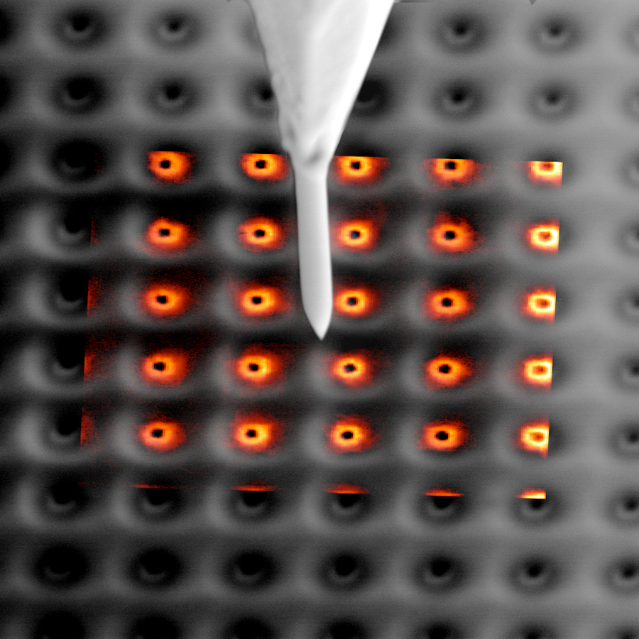
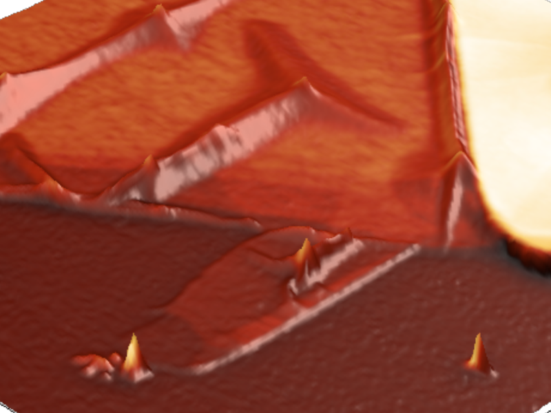
Failure analysis of a NAND structure
Using AFM-in-FIB/SEM, specific vias in a NAND structure were identified, sequentionally delayered using PFIB and analyzed via Conductive-AFM mapping (C-AFM) and I/V spectroscopy.
This approach provides real-time monitoring of the delayering process, ensuring accurate via targeting and revealing electrical failures of the nodes at different depths.
Failure analysis with AFM-in-FIB/SEM begins with site-specific sample preparation using FIB to expose to the defect area. The AFM tip is then navigated to the region of interest for high-resolution electrical characterization, such as C-AFM or SSRM. Results are correlated (calibrated if needed) with SEM techniques for a comprehensive failure understanding.
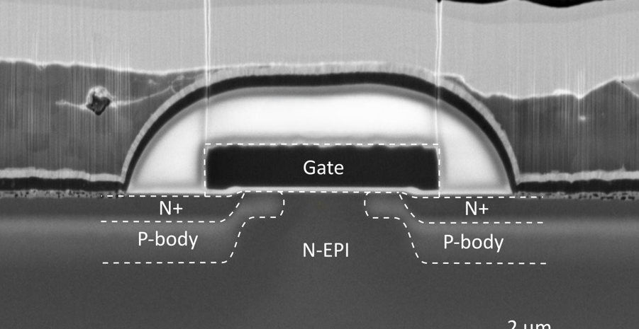
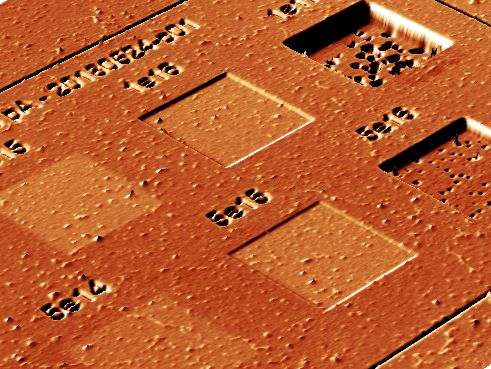
Dopant Concentration Analysis of MOSFET Transistor
We analyzed dopant concentration in semiconductor devices using Scanning Spreading Resistance Microscopy (SSRM) combined with SEM for high-resolution, site-specific electrical characterization.
In-situ SEM-SSRM measurements provide efficient workflow for dopant concentration mapping with nanoscale precision. By correlating SEM imaging with local electrical properties, we can identify variations in doping levels critical for device performance and reliability.
For SiC MOSFET transistors, this approach enables direct characterization of doped layers and junctions analysing their precise shape, size, and repeatability of the structures, which has a crucial impact on its functionality and MOSFET performance, ensuring proper conductivity and minimizing losses.

Webinar

Ready to discuss your own application?

Inside the Chip: Semiconductor Failure Analysis with AFM-in-SEM

In-Situ SEM Masterclass at QUT University!

Upcoming Battery Webinar | Unveiling Battery Electrode Secrets with AFM-in-SEM