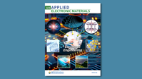
Impact of Electron Irradiation on WS2 Nanotube Devices
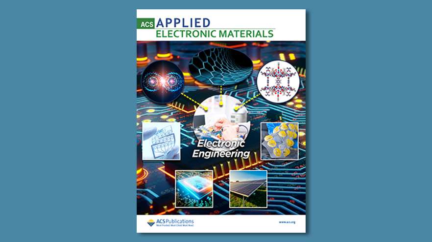
Uncover the hidden effects of electron beam exposure on WS2 nanotubes and learn why understanding substrate charging is crucial for accurate prototyping and reliable device performance in next-generation electronics.
Scientific articles
|
17. 12. 2024
|
by ACS Applied Electronic Materials
Material Science
Technology
Related articles
Scientific articles
|
12. 03. 2025
|
by Phys. Status Solidi A
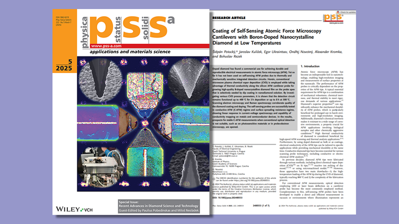
AFM-in-SEM LiteScope on the Cover of a Key Study on Diamond-Coated Probes
Material Science
Technology
Scientific articles
|
18. 11. 2024
|
by Materials
Enhancing Thermoplastic Starch with Maltodextrin: Key Properties and Performance Insights
Material Science
Technology

Scientific articles
|
12. 08. 2024
|
by Scientific Reports
3D Surface Roughness Measurement of Core–Shell Microparticles
Product
Technology
Scientific articles
|
25. 06. 2024
|
by Production Engineering
ZrN coating as a source for the synthesis of a new hybrid ceramic layer
Product
Technology

Scientific articles
|
28. 02. 2024
|
by Beilstein J. Nanotechnology
Advancements in graphene nanopatterning using focused electron-beam-induced etching
Product
Technology

